Electrostatic carrier doping is a technique that carriers (electrons or holes)
are induced into interface (channel region of semiconductor) between semiconductor and gate dielectric by applying bias voltage to gate
dielectric. This technique enables carriers to be accumulated into target materials without any doping of atoms. In general transistor,
small amounts of carriers (~1/100 per molecule or atom) are accumulated into the channel region of semiconductor by using this technique,
while more than one per molecule or atom may be necessary for a modification of physical properties of materials. Recently, physical
properties were controlled in some of inorganic materials by electrostatic doping technique with electric double layer (EDL) capacitor.
By use of this technique, Prof. Iwasa group (Univ. Tokyo) succeeded in induction of superconductivity in SrTiO3, ZrNCl,
KTaO3….. Thus, the electrostatic doing becomes an important way for making superconductors. Since the carriers are
accumulated only in channel region (~1 nm) which contacts (connects) to gate dielectric, the induced superconductivity may
be two-dimensional (2D) which is very attractive from physics point of view. We are trying to apply the electrostatic doping
technique to 2D organic materials and inorganic materials. Currently, we are applying this technique to FeSeTe systems and
topological insulators (ex. Bi2Se3) to modify their physical properties. Our group succeeded in carrier accumulation into
FeSe1-xTex by this technique. The topological insulator, in which metallic surface state coexists with bulk
band-insulating state, provides an interesting stage for electrostatic carrier doping, because the feature of surface state
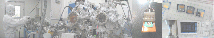
may be electively extracted by electrostatic doping. Our group has facilities required for experiments of electrostatic doping
in a wide temperature region. |